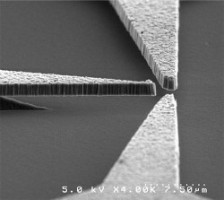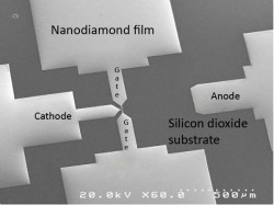
There is a new way to design computer chips and electronic circuitry for extreme environments: make them out of diamond.
A team of electrical engineers at Vanderbilt University has developed all the basic components needed to create microelectronic devices out of thin films of nanodiamond. They have created diamond versions of transistors and, most recently, logical gates, which are a key element in computers.
“Diamond-based devices have the potential to operate at higher speeds and require less power than silicon-based devices,” Research Professor of Electrical Engineering Jimmy Davidson said. “Diamond is the most inert material known, so our devices are largely immune to radiation damage and can operate at much higher temperatures than those made from silicon.”
Their design of a logical gate is described in the Aug. 4 issue of the journal Electronics Letters. Co-authors of the paper are graduate student Nikkon Ghosh, Professor of Electrical Engineering Weng Poo Kang.
Not an engagement ring

Davidson was quick to point out that even though their design uses diamond film, it is not exorbitantly expensive. The devices are so small that about one billion of them can be fabricated from one carat of diamond. The films are made from hydrogen and methane using a method called chemical vapor deposition that is widely used in the microelectronics industry for other purposes. This deposited form of diamond is less than one-thousandth the cost of “jewelry” diamond, which has made it inexpensive enough so that companies are putting diamond coatings on tools, cookware and other industrial products. As a result, the cost of producing nanodiamond devices should be competitive with silicon.
Potential applications include military electronics, circuitry that operates in space, ultra-high speed switches, ultra-low power applications and sensors that operate in high radiation environments, at extremely high temperatures up to 900 degrees Fahrenheit and extremely low temperatures down to minus 300 degrees Fahrenheit.

Hybrid of old and new
The nanodiamond circuits are a hybrid of old fashioned vacuum tubes and modern solid-state microelectronics and combine some of the best qualities of both technologies.
Nanodiamond devices consist of a thin film of nanodiamond that is laid down on a layer of silicon dioxide. Much as they do in vacuum tubes, the electrons move through vacuum between the nanodiamond components, instead of flowing through solid material the way they do in normal microelectronic devices. As a result, they require vacuum packaging to operate.
“The reason your laptop gets hot is because the electrons pumping through its transistors bump into the atoms in the semiconductor and heat them up,” Davidson said. “Because our devices use electron transport in vacuum they don’t produce nearly as much heat.”

This transmission efficiency is also one reason why the new devices can run on very small amounts of electrical current. Another is that diamond is the best electron emitter in the world so it doesn’t take much energy to produce strong electron beams. “We think we can make devices that use one tenth the power of the most efficient silicon devices,” said Davidson.
The design is also largely immune to radiation damage. Radiation disrupts the operation of transistors by inducing unwanted charge in the silicon, causing an effect like tripping the circuit breaker in your home. In the nanodiamond device, on the other hand, the electrons flow through vacuum so there is nothing for energetic particles to disrupt. If the particles strike the nanodiamond anode or cathode, the impact is limited to a small fluctuation in the electron flow, not complete disruption, as is the case with silicon devices.

“When I read about the problems at the Fukushima power plant after the Japanese tsunami, I realized that nanodiamond circuits would be perfect for failsafe circuitry in nuclear reactors,” Davidson said. “It wouldn’t be affected by high radiation levels or the high temperatures created by the explosions.”
Nanodiamond devices can be manufactured by processes that the semiconductor industry currently uses. The one exception is the requirement to operate in vacuum, which would require some modification in the packaging process. Currently, semiconductor chips are sealed in packages filled with an inert gas like argon or simply encapsulated in plastic, protecting them from chemical degradation. Davidson and his colleagues have investigated the packaging process and have found that the metallic seals used in military-grade circuitry are strong enough to hold an adequate vacuum for centuries.
Watch webcast of Davidson talking about the first nanodiamond vacuum emitter device logic circuits.
The research was supported by grants from the U.S. Army.